Next: 9 Integrated Software View Up: Appnotes Index Previous:7 Architecture Design Process Detailed Description
![]()
![]()
![]()
![]()
Next: 9 Integrated Software View
Up: Appnotes Index
Previous:7 Architecture Design Process Detailed Description
We start the module design process with inputs in the form of the Module Requirements Specification generated by architecture design. The module is the fundamental line-replaceable unit (LRU) for the signal processor hardware. It is the primary focus of testability, reliability, and maintainability analyses.Here the module architecture is partitioned into a combination of existing components and new or existing ASICs. The ASIC design process is spun off at this point as another mini-spiral in the risk driven development process.
ASIC design takes the Type C specification from architecture design, which may have been augmented by module design, and develops behavioral or RTL models of the ASIC using VHDL. This is followed by functional behavioral simulation. Next, we perform detailed design (synthesis) of the ASIC functional blocks, followed by gate-level functional simulation, using the same test vectors and expected outputs as in the behavioral simulation. The behavioral and gate-level simulations must agree 100 percent before proceeding to the next step.
In parallel with ASIC design, we perform the detailed module design involving interactive logic design, simulation, and timing analysis. Functions are partitioned to FPGAs, if applicable, and FPGA design begins as another mini-spiral.
We perform the first module-level simulations using the ASIC behavioral or RTL model(s) developed by the ASIC designers. As the ASIC design progresses, gate-level ASIC models, and FPGA models may be brought into the overall module simulation environment, depending on overall module complexity. A test bench that is usually generated by architecture design is used on the module as a check for correct requirements mapping and implementation. We then perform timing analysis and fault simulation. When the module is deemed correct (functionally and in terms of timing), after the Module Preliminary Design Review, module preliminary design is complete.
FPGA design, also in parallel with module design, involves the development of a programmable logic device from its beginning as a behavioral VHDL model through detailed design, synthesis, place and route, and programming using a device programmer. This process is similar to the ASIC design process.
We start final module design with the physical layout. We back-annotate added signal delays due to module routing to the simulation model, and the perform a complete module simulation. In some cases, we simulate multiple modules at the structural level to test interfaces and a higher level of functionality. The test bench used to stimulate a multimodule simulation is the same as for earlier behavioral simulations. After the Pre-Release Design Review, manufacturing fabricates and assembles the first-piece module and engineering tests it, using the same test vectors used during module simulation. The Final Design Review is held, after which all module documentation is signed off.
Backplane design, which began in parallel with module design, involves determining the intermodule wiring scheme (printed wiring board and/or wirewrap) for the collection of modules, and performing detailed analysis of the signal integrity of the backplane, using transmission line and crosstalk analysis tools.
Chassis design also begins in parallel with other design activities and encompasses the mechanical and electrical design and analysis of the structure that holds the backplane(s), power supplies, cable and harness, I/O connectors, and other miscellaneous hardware. With appropriate CAD tools, the chassis is designed and a 3D model is generated. This model is used to analyze stress, temperature, mechanical tolerances, and dynamic characteristics.
Also in parallel with module and ASIC design, we re-evaluate the chassis mechanical conceptual design approach against the program subsystem-level requirements (B2) specification. We develop a mechanical design concept for the enclosures and electrical packaging, then generate solid models and a C-level specification. This effort requires support from manufacturing for producibility and cost trade-offs. Producibility analysis is built into the mechanical design's early stages. The Preliminary Design Phase refines the chassis design concepts developed during the Conceptual phase. We generate and integrate solid models and detail layouts, where applicable, into overall mechanical design layouts that incorporate key features, interfaces, dimensions, etc., for the particular mechanical design. This reduces risk due to misinterpretation or missed revisions, and provides the up-front discipline and integration to assure a correct initial database during the Preliminary Design Phase. A Preliminary Design Review (PDR) is held following completion of preliminary design and prior starting detail design. At this point, we have completed all detail and interface layouts, selected major parts, identified materials and processes, and completed and analyzed major chassis models. We begin preparing test plans and issue long-lead parts lists to manufacturing. The PDR ensures that these tasks have been satisfactorily completed, preliminary design is complete, and detail designs can be generated from the preliminary design.
In the final design phase for the chassis, we generate the actual detail design and assembly drawings used to fabricate and assemble hardware end-items. Designs are transferred electronically from solid models into 2D or 3D formats used to fabricate hardware without unnecessary modification. Outputs for the Final Design Phase include issue of Release Packages that allow manufacturing and sourcing to efficiently fabricate or procure hardware. A Final Design Review (FDR) is held before issue of the Release Packages to ensure that hardware designs are correct and meet the requirements of the subsystem level specification. The major portion of the mechanical engineering effort is complete following the FDR and issue of Release Packages.
Subsystem integration and test is the last process in the overall hardware design process. We follow a phased integration approach where we integrate fully-tested individual pieces into the next higher level. Initially, we integrate the modules into backplanes, then test them; the tested backplanes are then integrated into frames and tested. The eventual result is a complete, fully tested subsystem. Detailed test procedures are followed in all phases of this process.
We review the test requirements, testability goals, BIT requirements, and target tester for this module. This step includes fault coverage goals, fault isolation goals, identifying replaceable units (RUs), type of testing to be performed (i.e., functional, in-circuit), type of test machine that will test the module, design-cycle time, tester-cycle time, level of test (module, system), and information on any standard test busses that may be required for the system.
Another important aspect of testability goals is whether and how a circuit must be probed. For example, it may be acceptable to probe a board in factory test (before conformal coat), but probing may not be allowed for field test. It is important to know and analyze all these constraints and requirements before developing a testability concept and plan.
We generate a concept for designing-in testability for this module. As we identify the test objectives, we select the best method for implementation, such as off-line (external stimulus and response), built-in (internal stimulus and response), and self-checking (e.g., parity checking during operation). The output is a preliminary testability concept document that the designers use when performing the detailed electrical design.
We may need to conduct trade-offs with architecture design and backplane designers following this analysis to achieve the desired module requirements. Manufacturing and mechanical engineering should be involved to ensure that the proposed design can be produced within project, technology, and cost constraints. Reliability and maintainability engineering should be consulted so that the overall architecture and parts chosen meet reliability/maintainability needs. Sourcing should be notified of any possible long-lead parts selected to determine if the procurement time for these devices meets schedule constraints.
The first step in designing a behavioral model of a module is to finalize and define, in detail, the interconnections between functional blocks in the block diagram of the module. After we define all the I/O to each functional block, we can then develop the behavioral model for the function or further break the function into smaller blocks. Incomplete interconnection definition increases design time and increases interdependence of functional block designs. A module requiring multiple design engineers should have very accurate inter-block definition; changes of I/O should be immediately documented for hand-off and future review.
When developing the behavioral model, the module design engineer should reflect the inherent structure of the design. If, for example, the module has a pipelined architecture, the pipelines and the functions performed by each pipeline stage should be evident from the model. The purpose is to produce a model with sufficient detail to guide gate-level design.
The design database is continually updated with more detailed descriptions of each function as the information becomes available. The I/O definition of each block is detailed enough to allow independent, concurrent design of each function. We then compare functions to the reuse library functions to eliminate duplication of effort. We enter new, common behavioral models into the library database as they are developed and validated.
Also included in this step is development of the 'tester' model, which applies input vectors to the model and collects and analyzes the results. This is a simple model written in the same language as the behavioral model or a complex suite of programs integrated into a complete simulation environment.
Generating test vectors for a module generally involves more than just specifying bit patterns. In most cases, we must define a 'tester' logic function to generate stimuli to emulate, for example, a bus interface protocol. When a standard microcomputer is involved, the test vectors are limited to the relatively small number of signals needed to reset the processor, plus the (sometimes extensive) firmware that must be downloaded to RAM for subsequent execution by the processor, which in turn generates bus activity, etc.
There are generally two classes of test vectors: functional and production. Functional test vectors verify that the design works as intended. Production test vectors differ from functional vectors in that the production vectors detect manufacturing defects. The functional vectors may also be used as production vectors, but are usually augmented with additional vectors to detect module faults that the functional vectors do not reveal. Production test vectors generally also use any designed-in-test features of the design, such as controllability and observability points and boundary scan. These vectors must also consider the target tester's restrictions, which include simulation speeds, timing limitations of the tester's drive and detect channels, pattern length, and pattern depth.
In this step, we emphasize generating functional test vectors, although some attempt at vectors designed for fault detection can be made. In "Perform Fault Simulation," the designer grades the vector set on its ability to detect module faults. Additional vectors needed to increase fault coverage will be produced in that step.
We perform this step concurrently with "Perform Functional Simulation." As we develop each group of test vectors designed to test a specific function on the module, the simulation is usually run using that group to verify the function instead of generating all the test vectors before running any simulations.
The module designer considers all available options before proceeding with the design process. If the library search produces an existing module that meets the requirements, no further analysis is needed. If an exact match is not made, we can check the library for other designs that could be used, either whole or in part. The library also contains entries that make it possible to contact the original designers, who could be valuable consultants. We use the results from this review of existing designs and the cost goals to determine the actual module design approach.
The Module Requirements Specification, generated primarily during architecture design, is a high-level description of the module being designed. We can generate it after completing a firm definition of the architecture. This document should include the following minimum subset of topics:
The module electrical design process presented here assumes that we will simulate modules after the logic schematic is fully captured or the logic synthesized and a netlist generated. A more structured, top-down approach can also be accommodated. The following steps can either be completed for the full design, as shown, or they can be repeated as each functional block of the design is generated during the functional requirements generation step. If a behavioral model was generated previously, mixed-level simulations can be run as the logic for the different functional blocks is generated.
As the detailed design progresses, it should be captured with the appropriate schematic capture tool.
If architecture design specified the use of any ASICs, any additional ASIC requirements must be provided to the ASIC designers in the form of additions to the ASIC Requirements document produced by architecture design.
We must now refine the testability features of the module introduced in the conceptual design. Additional hardware may be required to provide for testing of all functions.
Information is also required regarding the target module tester. This data minimizes the amount of translation required when the production test vectors are generated. This data should include information about restrictions on device names, signal fan outs and loading, and power and ground pins (for standardization of test fixtures).
Representatives from mechanical engineering and manufacturing should be consulted during this step. The mechanical engineer can help with power dissipation and the distribution of heat across the module. These issues can affect parts placement. Manufacturing and mechanical engineering can handle other concerns related to parts placement, such as the minimum distance parts can be placed from each other, and the positioning of Pin Grid Array (PGA) devices so that solder inspections can take place.
We begin the timing analysis by identifying the design's critical paths. A path for this analysis is the set of wires and components between any two pins in the design. A timing path is one that begins at the module's primary inputs or any internal register's outputs and ends at the module's primary outputs or any internal register's inputs. The path delay is the accumulation of propagation times through each wire and each component on the path. Note that the propagation delay through a component is not a constant, but is a function of the capacitive load on the driving pin. The critical paths of a design are the set of timing paths that have the greatest path delay values, and thus determine the limit of the design's timing performance.
We use a static timing analyzer for timing analysis in this step. The static timing analyzer differs from a simulator primarily in that the analysis is independent of the stimulus applied. A static timing analyzer determines the path delay for every timing path in the design, and analyzes each for timing violations similar to those identified by the simulator. Timing problems are identified by timing violation reports. One advantage of the static timing analyzer versus the simulator is that it identifies timing problems and critical paths that are not sensitized by the input stimulus. A disadvantage is that it often reports many false timing errors that would not occur in the actual module.
Critical path analysis using a static timing analyzer provides a quick approach to finding timing problems in the design, such as setup or hold time violations. It does not find all timing problems, especially those involving complex CPLD or controller designs. A worst-case timing analysis that uses a comprehensive set of functional test vectors may be required to broaden the timing analysis.
Loading analysis determines the electrical loading on the outputs of module devices, and includes DC and AC components. A device's DC loading is affected by DC current from other devices that flow through its output. A device's AC loading is related to the capacitance presented to its output due to the capacitance of other devices and interconnections connected to it. Excessive DC loading can cause power dissipation to exceed device specifications; excessive AC loading can cause timing problems and signal distortion.
We send the results of the analyses to various other members of the overall subsystem team: thermal analysis data to mechanical engineers involved in the design of the cooling system; and power and loading data to the backplane designer specifying power supplies and interconnecting modules in the system.
The purpose of this step is to simulate the module to test its basic functionality, using the previously-generated test vectors. ASICs, if present, will be modeled behaviorally or with hardware models. We use worst-case timing values for all components. We also broaden the timing analysis by performing a worst-case minimum/maximum timing analysis using test vectors and the simulator.
For the timing analysis, we use the simulator to simulate the minimum and maximum delays of components simultaneously. When an input to a component changes, two transitions are scheduled on the component outputs. The first transition is to an unknown state and occurs with the minimum propagation delay. The second transition is to the final state, which occurs with the maximum propagation delay for the component.
Simulation output reports all functional timing hazards, such as setup and hold-time violations, illegal edge violations, and excessively 'long' signal paths based on user specifications. Also reported are structural timing hazards (circuit problems arising from the structure of the circuit).
Once the gate-level design is complete, we must verify the accuracy of the design. The first step is to perform a gate-level functional simulation. This is similar to the behavioral model functional simulation performed previously, except that we use the gate-level design database for simulation rather than the VHDL model. The functional simulation is also concerned with the timing of the gate-level design. The purpose is to verify the functional correctness and timing of the logic.
Mentor's QuickSim II has a mixed-mode capability that allows VHDL and gate level representations to be simulated in the same design simultaneously. Because of this, it will probably be common to perform this step in parallel with the interactive logic design. We compare the output of the detailed gate-level simulation with the previously-verified behavioral simulation to determine the functional correctness of the detailed design. We must isolate discrepancies between the two models and correct them until both simulations produce the same results.
We can design a subset of the entire VHDL model at the gate level and verify it using the test vectors we developed during the behavioral model functional simulation. Once this function is verified, we design the next function at the gate level and verify it, and so on until the entire design is complete.
The results of a fault simulation often indicate design areas that are inadequately tested and that require additional or modified stimulus to fully test. We use this information to create an adequate set of test vectors to fully test the module and also to identify a reasonably small set of potential failures through the fault dictionary. The test engineer who constructs the module test program uses these vectors, and the associated fault dictionary, to construct the test program concurrently with the module design.
The fault simulation process involves running multiple logic simulations, but each simulation has a fault introduced into the design before it begins. If the response from the faulted simulation differs from the response of the ideal simulation, the fault is either detected or potentially detected. The fault is detected if the response of the ideal simulator was a ' 1 ' while the response of the faulted simulator was a ' 0 ' or vice versa. The fault is potentially detected if either simulator's response was unknown while the other was known. The fault coverage is the percentage of all faults that are detected.
Many types of faults, such as opens, shorts, and faults internal to components, are possible in the physical module. It is impractical to simulate all types of possible faults, so we usually limit a simulated module fault to a pin on the module that is grounded or connected to power.
If the fault coverage for the set of test vectors does not meet project requirements, we generate additional test vectors to meet the requirement.
A designer should include at least the following data items:
We use a transmission line analysis tool at this point. This tool predicts delays, waveform distortion, and ringing due to transmission line effects. Crosstalk, the coupling of signals from one interconnection path (net) to another, is also evaluated with a suitable tool. The engineer can correct these problems by adding terminations, changing parts placement, and making other changes. We must evaluate the impact of any design changes on the module's cost, manufacturability, reliability, and testability.
Also in this step, we produce the test database, which is the set of test vectors/expected responses in the correct format to drive the module tester. If the simulation is properly designed, in this step we simply reformat the existing simulation vectors. It is therefore important to design the simulation so that the simulation vectors can be easily used for module test.
We use the module test procedure and module test database, along with the post-processed vectors, to generate the necessary files and procedures for the target tester. We then verify the test program on the target test system. Any changes that may be necessary are reflected back into the module test procedure and/or simulation database. Any conceptual changes are noted in the Testability Document and the Design-for-Testability Design Review Checklist, if necessary.
We evaluate the estimated module recurring engineering costs against cost goals and report actual productivity data at the review.
Fabricate First-Piece Module - Manufacturing or an outside supplier fabricates the first-piece module.
Assemble First-Piece Module - We assemble the first module by inserting components in this step.
First-Piece Module Engineering Test - During this step, we test the first module using the module test equipment according to the test procedure document. We perform design verification in which we check timing, performance under variations in voltage and temperature, and other design performance criteria. Design verification determines if the design will meet environmental requirements. If any problems with the design are discovered, the module design engineer makes any design changes needed to correct them.
We test and characterize the module on an automatic tester. All tests are performed over the full voltage and temperature ranges. Module characterization measures all electrical parameters. We analyze the data to determine module quality and capability.
The ATE test vectors used in the functional and parametric tests are finalized to incorporate any adjustments needed to satisfy module, adapter, and tester interfacing anomalies. We analyze module test results to determine the integrity of the module-to-tester interfacing.
Update Documentation and Release Package - The first-piece module engineering test may reveal deficiencies in the design that need to be changed. If this is the case, then a documentation and Release Package update is needed.
Conduct Final Design Review - The FDR is the last design review of the completed engineering drawing package for the module. We check all details of the engineering documentation being released. This review is crucial, because any errors/discrepancies in the release package that are not found will affect production of the final system. There may be a large number of this type of module in a system, so the effects of an incorrect release package can be great.
Engineering Signoff - After the FDR, engineering signs off the drawings for release to the drawing system. The module design cycle is now complete.
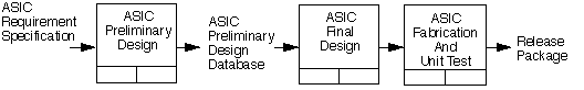
In the third phase, we fabricate and test the chip with the ASIC supplier. The ASIC design process is detailed in Figure 8 - 2.
Critical to success of the ASIC design process is generating an accurate specification, following DFT practices, performing multi-level simulations, and conducting thorough design reviews.
We may have to conduct tradeoffs with architecture and module designers following this analysis to achieve the desired ASIC requirements. Manufacturing and mechanical engineering should be consulted to ensure the proposed design can be produced within project, technology, and cost constraints. Reliability engineering should be involved, along with the supplier, to ensure that the fabrication process and packaging meets specified reliability requirements. The test engineer can provide information on the IC tester requirements and limitations.
When developing the behavioral model, the ASIC designer should reflect the inherent structure of the design. If, for example, the ASIC has a pipelined architecture, the pipelines and the functions performed by each pipeline stage should be evident from the model. The purpose is to produce a model with sufficient detail to guide gate-level design.
In this step, we also develop the 'tester' model, which applies input vectors to the model and collects and analyzes the results. This may be a simple model written in the same language as the behavioral model, or a complex suite of programs integrated into a complete simulation environment.
If additional logic is developed in this step, the ASIC designer updates the behavioral model to reflect the new functions, and develops additional test vectors to test the new logic. These vectors, combined with the behavioral vectors, form the nucleus of the final set of test vectors for the chip, and fully exercise all functions of the chip. The updated behavioral model is sent to the module engineer for module simulation.
We use a simulator that has a mixed-level capability that allows VHDL and gate-level designs to be simulated in the same design simultaneously. Because of this, it will probably be common to perform this step in parallel with the interactive logic design and synthesis. We can translate a subset of the entire VHDL model to a gate-level netlist and verify it using the test vectors developed during behavioral model functional simulation. Once this function is verified, we can translate the next function and verify it until the entire design is complete. The final gate-level design produces the same results as the behavioral model for a given set of test vectors.
In this step, we assume accurate timing information is available from the supplier, including loading and wire length estimates. In addition, many suppliers have special macrocells or megafunctions as part of their cell libraries. To perform accurate timing analysis at this stage in the design cycle, the timing analyzer must have access to the timing information for any supplier specific functions. If this is not the case, it may be necessary to delay this step until after the design has been translated to the supplier format.
Since the timing results from this stage are only estimates, the designer should not attempt to squeeze the last nanosecond out of the chip performance in this step. The purpose is to identify obvious problem areas, and make the changes necessary to get the performance as close to the requirements as possible. The detailed timing analysis will be done on the supplier toolset.
There are usually be two types of changes required to increase performance. The first type is fine-tuning the gate-level design, such as replacing a carry look ahead adder with a carry select adder. We can make this type of change to the netlist only, since the basic structure and functionality are not affected. The second type of change is a major architectural restructuring, such as adding a pipeline stage. We make this type of change to both the netlist and the behavioral model. In both cases, we rerun the functional simulation to verify that the changes did not affect the functional operation of the design.
The exact set of requirements varies according to the supplier, but the following additional simulations are commonly required. Design verification simulation checks the design for proper design rule use. A test file is usually produced that converts the test vector set into a format compatible with the supplier's test facility. A toggle test verifies that the vector set toggles every net in the design at least once. The parametric simulation is used to verify proper voltage levels and/or drive current in the I/O signals.
If the performance does not meet the requirements, the designer makes changes and sends the new netlist back to the supplier for layout. This process continues until the performance is acceptable.
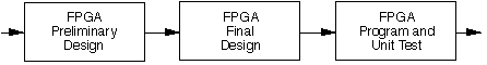
The FPGA process described here is kept generic intentionally and may be applied to various classes of programmable logic devices including Field Programmable Gate Arrays, Complex Programmable Logic Devices (CPLDs), and Erasable Programmable Logic Devices (EPLDs). The inputs to the FPGA process are a Requirements Specification, which usually is a part of a higher-level module (board) Requirements Specification and a VHDL behavioral model of the FPGA function. Major outputs from the process are a fusemap used to program the device and test vectors used to verify the functionality of the design. The design can be divided into three phases: Preliminary Design, Final Design, and Programming and Unit Test. These phases depicted in Figure 8 - 3 are described in the following paragraphs.
Three styles of design entry using VHDL are possible: behavioral, Boolean, and structural. Tabular descriptions are also possible. A complex VHDL design can be built by successively combining building blocks in related layers. Up to this point the designer has not implied any particular hardware. The assumption is that he has captured the scope of the design into one abstract level VHDL description. This description may be realizable in a broad range of hardware devices. Memory, interface, microprocessor, one or more programmable logic devices, and a variety of other integrated circuits may be required to realize the design. Therefore, the design must be decomposed into those specific devices which the designer chooses for realization.
Using a CAE tool the designer can explore the variety of device implementations by interactively varying design criteria - including cost, preferred parts, device count, speed, and power - to find an optimum design solution.
Assuming that partitioning has been performed and a particular FPGA has been selected for a certain function, further decomposition tasks must be performed. Clocks may have to be connected to a clock distribution network and high fanout inputs must be connected to high drive input cells, if desired.
Functional Verification --- During this step the refined FPGA behavioral VHDL model is verified to ensure that it meets functional and performance requirements. This is accomplished by performing a functional simulation using the VHDL FPGA model. The Testbench used for this verification should be the set of test vectors passed down from module design or architecture design, usually augmented by the FPGA designer. Outputs from the simulation are compared to the expected values passed down from the module designer or architecture design.
Placement and Routing --- This step involves the actual placing and routing of the design into the actual device. The place and route software accepts the output of a technology mapper and generates a file for use by the programming equipment and a timing model for use by downstream analysis tools. The place and route determines the actual cell choice for each logic function to be implemented and the wire connections for the signals which pass and from the logic cells and I/O cells. Once the place and route is completed, a performance analysis is usually done to verify that the design will meet expected performance.
Functional and Timing Simulation --- After place and route of the target design, it must be resimulated with backannotated delays to verify that it still functions as expected. A full timing gate-level simulation model is assembled using the backannotation delay information. Test vectors generated for verifying the behavioral VHDL model are used to exercise the model. The resulting post-route simulation outputs are compared against the simulation results generated during the functional model verification. Once validated, the full-timing gate-level model can be made available for use in module-level simulations.
Fault Simulation --- A fault simulation can be optionally performed on the FPGA gate-level design to detect stuck-at-one, stuck-at-zero fault conditions. The procedures for this fault simulation are the same as those for the ASIC design process.
Refine Test Plans/Procedures --- The detailed test plan and test procedures for the FPGA are refined as necessary. The plan describes the method and the procedures define the step-by-step the instructions to be used to test the device standalone, before it is inserted onto a module.
Conduct Design Review --- This design review is optional, and usually is made part of the module design reviews. This review provides a detailed technical evaluation of the FPGA design function and performance, and serves as the focal point for identifying any outstanding issues. The design review is conducted in accordance with local policies and procedures. A detailed design package is generated by the designer for inclusion in a module-level design review.
There are several terms which are used interchangeably when describing backplanes; these terms include "backpanel" and "motherboard". Although "backplane" and "motherboard" are sometimes used to differentiate between wire wrap and printed wiring, respectively, there is no industry wide standard for these terms. This document will refer to "backplanes" only.
Commercial or Industry Standard backplanes, such as VMEbus or Multibus II, are backplanes which have been manufactured to a specification or standard, with some or all pins predefined, and are available off the shelf.
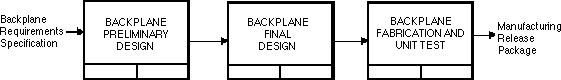
The backplane design process described here applies to the design of custom backplanes of varying complexities with wirewrap and/or PWB interconnections. It may also encompass the design of backplanes that use off-the-shelf or modified, off-the-shelf backplanes as the basis for a new design. The backplane design process flow is detailed in Figure 8 - 4.
Partitioning can significantly affect the size and complexity of a backplane. Poor partitioning can increase the number of layers and thus the cost of the backplane, while good partitioning can efficiently use the available space and minimize the number of layers or wiring. Poor partitioning can also lead to noise problems due to long signal runs or wire lengths.
A commercial/industry standard backplane fits the COTS philosophy. It requires no manufacturing time and minimal lead time, and a standard backplane can be chosen so that interface problems in a system can be minimized. It does, however, limit the user to the system functions that are provided in the standard.
Commercial or Industry Standard backplanes have many pins predesignated, and some that are user-defined. It is important for the designer to understand which of the pins are predefined by the standard, and which are left for the backplane designer to designate; obviously, the designer should not use any of the standard-defined pins for uses other than what the standard intended.
Detailed design work proceeds at this point, based on the design concept. This task includes input/output definition and the design of timing/control functions.
The purpose of this review is to ensure that the functional requirements of the backplane specification have been met. It will provide a detailed critical technical evaluation of the functional electrical design, and we will resolve any outstanding issues.
Once we have processed the wirewrap netlist, we route and level the wires using the user-specified rules for optimizing parallelism, line reflections, and wiring density. Wire routing entails searching for the optimum routing path while considering the electrical interaction of wires that were previously routed. For wires that fail the allowed criteria for parallelism, the design engineer can automatically convert the single wires to grounded twisted pair, or manually designate a different route for the wire.
After we complete routing and leveling for each wire, the wire connection list contains the necessary information to generate manufacturing tools.
Once the tools are generated, manufacturing uses the NC data and reports to assemble the backplane. Manufacturing either purchases or manufactures the bare board, and mounts the pins or connectors on the board. An objective of this step is to add the wire-wrapped wires to the backplane and, optionally, to test the wires as they are added to ensure that the proper connections were made. Depending on the design requirements, we test the backplane for continuity and isolation at various stages of assembly. It may be tested before wire installation, after initial hand wires and automatic wires are added, after all the wires are installed, or at all of those stages. Following the completion of this step, we test and debug the first-piece backplane.
Prior to chassis Preliminary design the mechanical and electrical designers review the proposal concept solution against the latest revised requirements. A new look is taken at the previous design and sub-contractors or co-contractors are consulted to explore the advantages of common approaches to packaging design and to determine that requirements that affect packaging have been met.
Items reviewed include layouts and solid models of major items, test plans, structural, thermal, tolerance, and weight analyses, source selections, updates to conceptual/proposal data, and interconnection layouts. We conduct this review in accordance with the local policy and procedure guidelines for internal design reviews, and following standard checklists. This step confirms that specifications can be met within established cost objectives, and should reconfirm the acceptability of designs and approaches generated in architecture design.
The top-level assembly is subjected to thermal, stress, EMI, shielding, dynamic, venting, weight, and other special analyses to assure that adequate margins have established to provide proper performance, even under worst case conditions.
We use the subsystem test plan as a starting point. For each test identified at the subsystem level, we attempt to define a similar test at the multichassis level, although this will not always be possible. As in the subsystem test plan, the multichassis test plans identify, in qualitative terms, the inputs, conditions of test, outputs, number of samples, etc., for each test. They also identify the test equipment required and how it will be used. Block diagrams of equipment configurations are useful to clarify their intended use.
We develop VHDL structural models for the VHDL behavioral models that were developed during the architecture design process. These structural models show the partitioning and interconnection of architecture component modules. We develop a test bench and a VHDL behavioral model for each module, and each module is, in turn, further decomposed and partitioned into other modules, macro-cells, MCMs, ASICs, or COTS components. We continue this iterative process of decomposition and partitioning for custom components until the hardware functions can be described as RTL logic transformations within leaf-level VHDL behavioral models. We can then automatically synthesize the leaf-level models into gate-level netlists. The VHDL models of programmable units are designed to interpret the data files produced by the software design process to facilitate hardware/software co-simulation and codesign. During the partitioning process, we can identify some of the modules, MCMs, and ASICs as custom parts, while others are selected from COTS parts. For custom-developed parts, we develop VHDL models down to the ASIC level, with a fully functional behavior and bus-functional model describing each ASIC. For COTS parts, we develop or obtain only VHDL behavioral models.
The VHDL behavioral models describe the timing and functionality of the module, macro-cell, MCM, and/or ASIC. Timing data includes:
Functionality data includes:
The test benches provide test procedures, stimuli, and expected results to verify that the design meets system requirements. The test benches are developed before, and are executed with, the behavioral models of the hardware designs during simulation. The design of test benches before component modeling supports the DFT methodology. The full-functional behavioral model forms the executable specification for a hardware design. We back-annotate the simulation results of the detailed hardware models to the higher level architecture models to make them precise.
Physical prototypes are designed, fabricated, tested and integrated with software per the program plan. The extent of the full system can range from a significant sub-assembly (i.e. a MCM or more typically a set of boards where each board type is present) to the complete system. Based upon these results the TSDs are updated with preliminary measurement data on fault population coverage. Design flaw data is collected based upon the extensive simulations of VP3 and the system prototype results. Preliminary results are collected on BIST coverage of manufacturing faults. If the program plan calls for a BIST demonstration, preliminary results are collected on BIST coverage of field support faults.
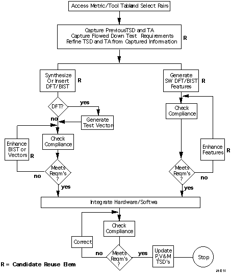
The generic test insertion process for each design entity is shown in Figure 8 - 7.
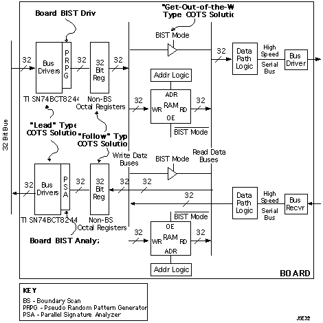
Testable COTS components should be used to the maximum extent practicable. In addition, the "Lead, follow, or get out of the way approach" to dealing with COTS is implemented. This involves adding, or using existing, DFT features to the design to deal with COTS. As illustrated in Figure 8 - 8, COTS devices possessing BIST features, such as the TI SN74BCT8244 (having a PRPG and PSA mode), are given a "lead" role, since they can lead a test process. COTS devices, such as the four non-boundary-scannable octal flip-flops are given the "follow role," since, while they cannot lead, they at least do not impede the BIST test flow originating at the boundary-scan octals. Finally, the RAM chips, being very complex, and having no test features, coupled with an inability to pass pseudorandom patterns through during RAM tests, must be relegated to the "get out of the way" role which means bypassing them during BIST mode using a output tri-stating approach.
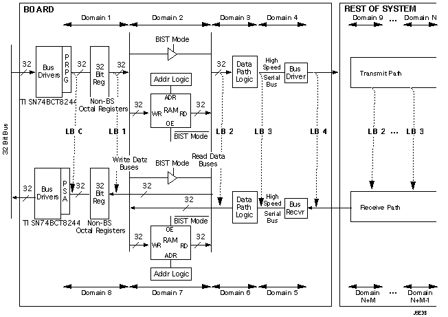
Test domain analysis is performed to stretch the reuse of all DFT/BIST structures. An example of this concept is shown in Figure 8 - 9. In the example, the source of BIST stimuli (8244) is analyzed to determine how much of the board (and eventually the rest of the system) can be tested using the PRPG and the PSA elements in the 8244s. A minimum of four domains (1 - 4) are covered along with additional domains in the rest of the system. By adding loopback capabilities, fault isolation is improved; and the number of domains covered is doubled. Pseudorandom patterns emanate from the source 8244 and responses through the loopback are compressed in the parallel signature analyzer in the sink 8244. Test domain analysis can be used to stretch the limits of reuse across packaging levels, as well as across the same package level.
Checking for compliance for COTS sections requires definition of the fault model, such that the coverage is measurable, using non-structural simulation models for the black box COTS elements or by using simplified functional fault models.
See the Design for Test application note for further details of the Detailed Design Step.
8.0 Detailed Design Process Detailed Description
We decompose the overall hardware design process into several distinct yet interrelated subprocesses:
8.1 Module/MCM Design Process
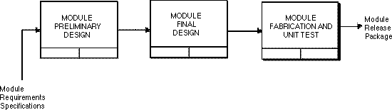
A module or MCM is a design that encompasses a logical function (or a group of logical functions) that can be implemented with circuit devices on a single circuit board. A module may include CPLDs/FPGAs or ASICs with their own design process. The module designer is responsible for the integrity of the outputs from these lower-level processes and for verifying their proper operation within the target digital module. The module/MCM design process is detailed in Figure 8 - 1.
8.1.1 Module Preliminary Design Phase
The module design process starts with preliminary analysis and review of the Module Requirements Specification. We search the RASSP design reuse library concurrently with the preliminary analysis after reviewing the module requirements. If no existing module meets the requirements, then we assess the feasibility of implementing the function and develop the overall architecture of the module. Sizing and partitioning the logical functions required on the module must be undertaken to:
8.1.1.1 Develop Module Behavioral Model
All modules are an integral part of a larger system and perform some unique subsystem function. In most cases, the architecture design engineer modeled the unique architectural elements using VHDL to gain confidence that all functional blocks will interact properly. In these cases, each partition (i.e., the module definition) should have had a high-level model developed that can be used by the module design engineer as the starting point for behavioral model development.
8.1.1.2 Generate Module Test Plan
We develop the Module Test Plan in accordance with local standards unless a different format is called for by the customer contract. The Test Plan should define all steps in the simulation process, including the strategy for generating test vectors that exercise all logic blocks, the method of performing comparisons with higher-level simulations, and the merging of ASIC behavioral and gate-level models and FPGAs into the simulation environment. The plan for meeting fault simulation stuck - at - 1 and stuck - at - 0 detection requirements is also addressed in this document. The Test Plan should be sufficiently detailed to allow efficient transfer of all information regarding the simulation effort to anyone associated with the module design. An informal peer review of the test plan is desirable to identify and correct any deficiencies in the plan before the start of simulation. Test engineering and manufacturing should be invited to the peer review.
8.1.1.3 Perform Behavioral Functional Simulation
We simulate the behavioral model of the module to verify that its performance meets the subsystem and ASIC requirements. This effort may be performed jointly by the module design engineer and the ASIC design engineer to ensure full coverage of all subsystem and module requirements. It is quite common for the module design engineer to discover design flaws in the module simulation that are difficult to detect in a single-chip simulation. This may include the detailed interaction of the ASIC during module reset or instruction abort procedures. Using the latest version of the ASIC behavioral model, the module design engineer can discover potential errors before module integration and test.
8.1.1.4 Generate Module Functional Test Vectors
A test vector is a set of bits used to test the operation of the module. In general, the bits define inputs to the module (stimulus) and the expected outputs from the module (response). As each vector is applied, the actual response of the module is compared to the expected response. If these match, the module is performing as designed. Test vectors are required for both simulation of the module and for testing the completed module.
8.1.1.5 Generate ASIC/FPGA Requirements
The module design engineer generates a high-level description of each function that is implemented as a FPGA. This description may include possible device types for implementation based on an evaluation of the approximate number of inputs, outputs, and product terms for each function. Both the module and FPGA designers review the FPGA requirements to ensure that the documentation is complete and consistent. Typically, the module design engineer and the FPGA design engineer are the same person.
8.1.1.6 Search Design Reuse
Concurrently with the preliminary analysis/design step, we search the RASSP design reuse library to determine if an existing (legacy) design can meet the requirements specified for the target module. In some cases, we can make a minor modification to an existing module to meet current requirements.
The detailed electrical design process involves the interconnecting the logic devices required to implement the module function. This portion of the process also includes placing the parts on the circuit board, analyzing module characteristics (Critical Path Analysis, generation of FPGA requirements, etc.), and producing a design database. This step is broken into sections explained in the following paragraphs.
8.1.1.7 Interactive Logic Design
We perform the detailed logic design of the module on each logic block concurrently, as appropriate. By designing each functional block separately, we can distribute the design of complex modules among multiple engineers to shorten the overall design cycle. However, each functional block must interface with its neighbors. Therefore, a functional block of the module cannot be considered an isolated design. Information must flow freely between the team of design engineers. Testability should be addressed at the start.
8.1.1.8 Preliminary Layout (Parts Placement)
After entry of the schematic into the workstation, we must do a preliminary parts placement to ensure that all devices in the design fit on the module. If there is insufficient room to fit the module function on the circuit board, then we must conduct trade-offs. These trade-offs can be alternative logic implementations using logic minimization techniques, using different part types (e.g., CPLDs), or repartitioning the module functionality to other modules.
8.1.1.9 Critical Path Analysis
The next step in the design process is timing analysis of critical paths. The purpose of the timing analysis is to analyze the timing performance of the design, primarily to determine producibility. Unlike the idealistic typical simulation, a real board is composed of parts whose timing performance varies from typical. In this analysis, we attempt to identify portions of the design where a set of fast or slow parts, or a combination of fast and slow parts, causes the board to function improperly.
8.1.1.10 Perform Power/Loading Analysis
Power analysis determines the module's electrical power requirement. There are maximum power specifications for a module, usually based on its size, which cannot be exceeded. If power specifications are not met, some high-power components may need to be replaced with functionally-equivalent, low-power devices.
8.1.1.11 Perform Functional Timing Simulation
We use simulation to confirm with a high degree of certainty that the first version of a module will function as desired without modifications. We can work our problems with the design on the simulation without the cost of producing a prototype, finding the problems, and reworking the module. We can also assess various design approaches without building a module.
8.1.1.12 Select Parts
This step is required to control parts usage on RASSP module designs. Prudent part selection by the module designer enables designers to take advantage of economies of scale in purchasing; it also enables lower inventory costs to the company and its customers. Procurement should be consulted for availability of long-lead items. Also, some new parts are introduced in the literature well before they are actually available for purchase. Procurement or the local components engineering group should be consulted regarding the availability of new parts. We must also consider the cost of parts chosen for the design to meet cost goals.
8.1.1.13 Generate Production Test Vectors
In most cases, we augment the functional test vector set used in functional simulation of the module to support fault simulation and the eventual needs of production test.
8.1.1.14 Perform Thermal Analysis
Thermal analysis identifies problems with heat caused by the power dissipation of the module components. Mechanical engineering sets requirements for heat distribution across a module, and if any areas on the module violate this requirement, we may need to move components to more evenly distribute the heat.
8.1.1.15 Perform Fault Simulation
A fault simulation indicates how well the stimulus tests the module's interconnections for manufacturing. It can also provide information on the set of potential failures based on a particular failure indication (e.g., pattern of incorrect outputs). The fault simulation provides this 'set of potential failures' through a fault dictionary. A fault dictionary lists faults for each output vector that would cause that output vector to fail. The intersection of all sets of potential failures for each failed vector indicates the set of potential faults on the module under test.
8.1.1.16 Generate Module Preliminary Design Document
The Module Preliminary Design document includes all information pertinent to the module design. This document has sufficient data for any engineer or technician who must later work with the module. For example, test engineers use it to debug the test program, and manufacturing uses it to repair boards.
8.1.1.17 Conduct Preliminary Module Design Review
After completing the module design and before committing the design to fabrication, we conduct the Preliminary Design Review. At a minimum, the project manager, the architecture designer, the module and ASIC designers attend. This review provides a detailed critical technical evaluation of the module design and resolves any outstanding issues. Testability features are evaluated. We review any ASIC or FPGA elements within the module. All disciplines that interact with module design should have representatives present at this review.
8.1.2 Final Design Phase
The final design phase addresses the transition from a functional design to a physical design. During this phase, we accurately place and route the module and analyze the parasitic effects of the module on signal integrity. The simulations performed address actual signal loading, signal crosstalk, line reflections, additional line delay, and skew. We finalize the test vectors and conduct the Pre-release Design Review before releasing the documentation and analysis results.
8.1.2.1 Module Place and Route
In this step, we determine the location of the parts on the module based on the preliminary placement completed previously. The interconnections between parts (routing) are also made. In some cases, we must conduct placement trade-offs due to routing concerns. We may have to move parts to minimize the length of critical interconnections such as clock lines.
8.1.2.2 Update Module Preliminary Design Document
We update the Module Preliminary Design Document and other related documentation to reflect the results of the behavioral simulation and the electrical analyses performed on the gate-level design. We add the final verified version of the behavioral model to the document. We also update other sections of the Preliminary Design Document that have changed. Such items may include the functional block diagram and other details that might have changed as a result of the modeling and analyses.
8.1.2.3 Perform Final Design Functional Timing Simulation
This functional simulation is identical to that performed in preliminary design, except that we use the design database back-annotated with layout parasitics for final verification.
8.1.2.4 Perform Final Design Thermal Analysis
This thermal analysis is identical to that performed in preliminary design, except that we use the final layout.
8.1.2.5 Perform Final Design Critical Path Analysis
This critical path analysis is identical to that performed in preliminary design, except that we use the design database back-annotated with layout parasitics for final verification.
8.1.2.6 Perform Production Timing Simulation
Module layout parasitics (trace length, number of vias traversed, signal crosstalk, trace parallelism, transmission line effects, etc.) can significantly effect module timing. This step allows the predicted delays caused by layout parasitics to be back-annotated to the simulator for a final simulation run that includes the best known timing information.
8.1.2.7 Generate Module Test Procedure and ATE Test Vectors
In this step, we generate the module test procedure document and test database. The test procedure contains the step-by-step procedure for testing the module. It includes such details as module tester setup, assignments of tester pods to module I/O signals, and filenames of test vector files. The information in the Test Plan produced previously can be included in this document. Test engineering and manufacturing should review the test procedure document.
8.1.2.8 Design and Build Test Adapters
The test engineer is responsible for specifying the electrical requirements for any hardware used to interface the module to the target test system. Depending on program requirements, this hardware may consist of either a totally unique design, or more generally, a generic test fixture design that is common to several module designs, plus unique interface hardware that provides module-specific signal routing, stimulus conditioning and output loads.
8.1.2.9 Generate Module Artwork and Manufacturing Tools
In this step we produce the tools for board fabrication. Artwork is used to generate printed circuit interconnection information. Other tools are needed to control equipment to drill holes in the boards, etc.
8.1.2.10 Prepare Module Release Package
We prepare the module drawing package, designated a 'Module Release Package.' This package contains all pertinent data for building the module and is released to internal manufacturing or an external supplier. The documentation package must fully specify the module to the manufacturing organization. It includes assembly drawings, logic schematics, parts list, and machine tool data.
8.1.2.11 Conduct Pre-Release Design Review
The Pre-release Design Review is the last design review of the completed design of the module before first-item production. This design review must verify that all architecture and module functional requirements have been met. We examine the results of all simulations and address any concerns, including all critical path and timing analyses, and all test-related issues, such as design-for-test and fault coverage. We check all details of the engineering documentation being released. The procedures to follow for this review are found in the local site Design Review Policy.
8.1.3 Hardware Fabrication, Assembly, and Test Phase
Engineering fabricates the first-item module, inserts components, and tests the module.
8.2 ASIC Design Process
This process, similar to module design, has three major phases. In the preliminary design phase, we generate a detailed specification for the device based on the architecture design effort. In this phase we develop, simulate, and verify a behavioral model, and develop a gate-level design (manually or via synthesis) and functionally-verify of the design via simulation. In the second phase, we translate the gate-level design to the supplier format, and perform all supplier-related simulations and pre-release procedures.
8.2.1 ASIC Preliminary Design Phase
We start the ASIC design process with preliminary analysis and review of the ASIC Requirements Document compiled by the architecture and module designers. We search the RASSP design reuse library concurrently with preliminary analysis after reviewing the ASIC Requirements Document. If the library search reveals that no existing ASIC meets the requirements, we assess the feasibility of implementing the defined ASIC, and develop the overall architecture of the ASIC. This includes defining and sizing a high-level functional architecture, defining the I/O interface signals, developing the instruction set architecture (when applicable), and defining special test features. Technological, packaging, and cost constraints are considered.
8.2.2 ASIC Final Design Phase
8.2.3 ASIC Fabrication and Unit Test Phase
8.3 FPGA Design Process
This section discusses the Field Programmable Gate Array design process which is becoming increasingly popular among designers of Digital Signal Processing hardware. This process has not been "re-invented" by the RASSP program, but rather reflects current industry standard methods and COTS tools.
8.3.1 FPGA Preliminary Design
Functional Design --- The purpose of this step is to refine an existing VHDL behavioral model of the FPGA function in sufficient detail so that it can be synthesized down to the specific programmable function unit level. The VHDL behavioral model is generally provided by the architecture definition process or by the module/MCM design process. The FPGA requirements document should contain the behavioral model, any requirements derived from module design, such as real estate restrictions, timing requirements, power restrictions, or any other module-related information.
8.3.2 FPGA Final Design
Logic Design / Synthesis --- After functional verification of the behavioral model the FPGA is synthesized from the refined behavioral model. Synthesis is the transformation of the design input at a high level of abstraction to a lower level. The VHDL description is turned into an unoptimized Boolean level description of the design. This unoptimized Boolean description is flattened, that is, it has no hierarchy and all intermediate variables are removed. At this point the design is not device-specific and is in a sum-of-products form. Next, the synthesized design is transformed into a device-specific netlist. This netlist is passed to the place and route tool.
8.3.3 FPGA - Program Device and Unit Test
After the FPGA or module design review, the devices can be programmed using JEDEC files that are downloaded to the device programmer. Then the individual devices can be unit tested using the same set of test vectors and expected outputs that were used during functional, timing, and fault simulations.
8.4 Backplane Design Process
The architecture design activity provides the basic requirements for backplane functions. The purpose of the backplane design process is to determine how to interconnect the modules to perform those functions.
8.4.1 Backplane Preliminary Design
We begin the backplane design process by forming a design concept, which is then documented in a Backplane Specification that describes how the backplane design engineer plans to implement the required functions. If the design concept calls for any new or modified modules, the backplane design engineer provides mechanical engineering with preliminary mechanical requirements at this stage. Backplane designs should, however, use previously-designed backplanes to the greatest extent possible.
8.4.2 Backplane Final Design
If the backplane design includes a PWB section, we perform the basic placement and routing steps as in module design. We perform a detailed electrical analysis to verify that proper design rules were followed in devising the interconnection scheme. We then generate artwork and tools for the PWBs, performed as in module design.
8.4.3 Fabricate, Assemble, and Unit Test Phase
8.5 Chassis Design Process
We define a chassis as the top-level hardware assembly containing the electronics and mechanical components of a subsystem such as a digital signal processor. A subsystem could be made up of more than a single chassis. Across the industry there is no standard terminology in this area. Other terms used to describe this hardware are "subassembly", "frame", and "box". A chassis usually contains at least one "backplane" which provides the interconnection for enclosed electronic printed wiring boards (also designated "modules" or "circuit card assemblies") as described in the following sections. The chassis design process can be broken up into two major phases which we designate Preliminary design and Final design. These processes are described in the following paragraphs and depicted in Figure 8 - 5.
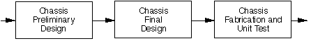
8.5.1 Chassis Preliminary Design
8.5.2 Chassis Final Design
The final design phase encompasses the detailed level mechanical design of the chassis. Detail design includes the interconnection cables and harnesses. These items require complete definition including, but not limited to: all dimensions and tolerances, material and finishes, marking requirements, test or acceptance criteria, etc. In this step, we begin the formal documentation of the chassis, the end product of which are drawings and parts lists necessary for a supplier or manufacturing to fabricate prototype or production hardware.
8.5.3 Chassis Fabrication, Assembly, and Unit Test
The bare chassis is manufactured and assembled locally or by an outside supplier. In either case, electrical and mechanical testing is performed according to the test plan and procedures developed previously.
8.6 Subsystem Integration and Test Process
In the overall RASSP design process, the subsystem (e.g., a signal processor) is usually the highest level of integration proposed. Subsystem integration and test is the last process the equipment undergoes. This process requires significant up-front planning in the form of integration plans, test plans, and test procedures long before the equipment is ready for actual integration and testing. Schedules for the availability of the tested subassemblies from the other design processes and manufacturing have to be negotiated. The subsystem integration and test process flow is detailed in Figure 8 - 6.
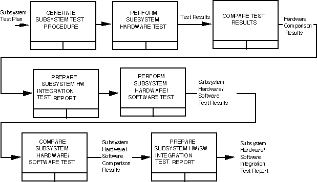
8.6.1 Generate Subsystem Integration Plan
In the first step in the subsystem integration and test process, we generate a subsystem integration plan. This plan lays out the events that will occur, and their order and timing, to achieve an integrated and tested subsystem within the cost and schedule allocated to this process. The integration plan defines the interactions and delivery schedules negotiated with other design activities and manufacturing. It also defines the state in which equipment will be delivered to this process.
8.6.2 Generate Subsystem Test Plan
In this step we generate a plan to test the integrated subsystem. This plan specifies all tests that must be performed to verify that the subsystem satisfies the B2 specification. The plan is driven by Section 4 (Quality Assurance) of the specification, which identifies the method (analysis, test, inspection, etc.) by which each of the requirements is verified. For each of these verification procedures, the test plan specifies the inputs, conditions of test, outputs, number of samples, etc., in qualitative terms. It also identifies the test equipment required and how it will be used. Block diagrams of equipment configurations are useful to clarify their intended use.
8.6.3 Generate Multichassis Test Plan
In large subsystems that have more than one chassis, an intermediate integration and test step between chassis test and full subsystem test is useful. This step develops the test plan for this multichassis test. There may be more than one of these multichassis tests. The goal is to integrate as few chassis as possible to make a subset of the subsystem that performs a testable function.
8.6.4 Generate Chassis Test Plan
In this step, we generate the test plan for the lowest level of integration that includes a testable unit. In most subsystems, this is the chassis level, although for some subsystems it is the backplane level. As in previous steps, the goal is to find and solve problems in the equipment as early in the test and integration process as possible. We generate a separate test plan for each unique chassis in the subsystem; again, these identify, in qualitative terms, the inputs, conditions of test, outputs, number of samples, etc., for each test. They also identify the test equipment required and how it will be used. Block diagrams of equipment configurations should be used to clarify their intended use.
8.6.5 Generate Test Procedures for Each Test Plan
In this step, we generate detailed test procedures from each individual test plan. Since these procedures are used for actual testing, they cover all testing configurations. However, test procedures do not normally specify the testing and debug approaches required to solve a problem when a test fails. The test plans and procedures should describe the purpose of the
test and how it functions in sufficient detail to make a debug approach apparent. The test procedures specify the test parameters outlined in the test plans. Expected outputs for each test and pass/fail criteria must be specified. Equipment figures and block diagrams from the test plans should be expanded and detail added. Forms should be included for each test which, when filled out, provide the basis for a test report.
8.6.6 Conduct Test Procedure Review
We review the test procedures to verify: (1) that the procedures accurately evaluate the subsystem's performance; (2) that the tests are done at as low a level in the design as possible; and (3) that the test procedures are complete. Incomplete test procedures have a significant cost impact on the testing floor. In addition to this internal review, many customers require approval of the subsystem level test procedures.
8.6.7 Integrate Backplanes and Test
This step is the first phase of actual integration and test. We integrate assembled and tested modules with the physical structure, backplane, and firmware into a testable chassis. We then use the test procedures developed for this configuration to test the equipment. In a large subsystem there may be several unique chassis tested during this step; each is tested according to its own unique test procedure. We use subsystem-level expected results generated in the architecture design process to verify satisfactory performance of the equipment. Following integration and test, we prepare a test report, and the tested equipment is then ready for the next level of integration. The next level of integration should not proceed until all tests have been completed and problems resolved.
8.6.8 Integrate Chassis and Test
This step is the second phase of actual integration and test. We integrate assembled and tested chassis with the physical multiframe structure into a testable multiframe configuration. In a large subsystem, there may be several unique multichassis configurations tested during this step; each is tested according to its own unique test procedure. In small subsystems there may not be a need for this level of integration and test. We use subsystem-level expected results generated in the architecture design process to verify satisfactory performance of the equipment. Following integration and test, we prepare a test report, and the tested equipment is then ready for the next level of integration. The next level of integration should not proceed until all tests have been completed and problems resolved.
8.6.9 Integrate Subsystem and Test
This step is the final phase of actual integration and test. We integrate assembled and tested multichassis configurations into the subsystem, which is then tested according to its test procedure. We use subsystem-level expected results generated in the subsystem design process to verify satisfactory performance of the equipment. Following integration and test, we prepare a test report, and the tested subsystem is then ready for further integration, if required.
8.7 Other Considerations in the Detailed Design Phase
8.7.1 Use of VHDL in the Hardware Design Process
The hardware design process transforms the architecture component VHDL models into detailed hardware designs. We decompose the abstract, non-evaluated architecture component models into full-functional VHDL models of their constituent entities. We use VHDL extensively throughout this process. In addition to the full-functional models, we create bus-functional models where needed to efficiently test interface designs. The bus-functional models are timing and functionally correct with respect to interface functionality only, whereas the full-functional models are correct with respect to both interface and internal function and timing.
- I/O timing constraints
- I/O interface structures
- I/O protocols
- Signal strengths
- Message types
- Data acceptance rate
8.7.2 Design For Test Tasks in Detailed Design
The focus of detailed design is synthesis and implementation of the selected architecture in hardware and software. From architecture verification, all boards have been broken down into behavioral blocks representing MCMs, ASICs, FPGAs or relatively small logic blocks (i.e. glue logic and/or functions to be implemented in PLDs). Major components such as processors, interconnects and sensor interfaces have been selected, specified and verified at least by simulation. Detailed design elaborates these designs into implementations by schematic capture, synthesis, place, route, autocode and primitive optimization activities.
![]()
![]()
![]()
![]()
Next: 9 Integrated Software View
Up: Appnotes Index
Previous:7 Architecture Design Process Detailed Description