Schematic Diagram and Source for Reference Design(DIGCAM)
Version 1.4
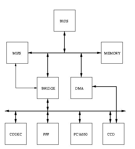
Block Diagram for Source 1.4
Source Code and Scripts
Steps to simulate/synthesize the design
Verifying the functionality of the design
Modifications from version 1.3
Description of the Reference Design
The Reference Design embodies the concept of a pre-designed,
parameterizable, de-configurable system-on-chip design.
Specifically, the reference design implements a Synopsys-synthesizable digital
camera. The camera is comprised of a MIPS-like micro-processor, a BIOS
for the processor, an ISA Bridge, a CODEC, a CCD pre-processor,
a DMA controller (Intel 8237A), a Programmable Parallel Port (similar
to the 8255 PPI), a UART chip (National PC16550), and memory. Various
parameters in these components may be programmed to analyze the
impact on the design metrics, namely power,
performance and chip area, for the individual component and the entire
system.
More Information on the motivation behind the reference design.
src32.tgz
Source Code and Script Files for 32-bit Peripheral Bus
Scripts for analyzing and synthesizing 32-bit design:
Source Code and Script Files for 8-bit Peripheral Bus
Available Upon Request. Please send e-mail to
dalton@cs.ucr.edu.
DIGCAM Assembler
dasm.pl is an assembler for programs written for the
DIGCAM's MIPS. The instructions follow the format of instr dest src1
src2. Please note that not all instruction require all fields. The
source code for the program currently contained in the BIOS is
code.asm. This demonstrates the format of the
DIGCAM assembly code. To use the DIGCAM Assembler the following command
should be used
dasm.pl asmfile > outfile
NOTE: Please note that dasm.pl is a Perl script and you must have a Perl
interpretter to use it.
- The first step is to analyze the different peripherals in the design. Type:
- vhdlan BIOS.vhd
- vhdlan BRIDGE.vhd
- vhdlan CCD.vhd
- vhdlan CODEC.vhd
- vhdlan DMA.vhd
- vhdlan MEMORY.vhd
- vhdlan MIPS.vhd
- vhdlan PC16550_SIM.vhd
- vhdlan PPP.vhd
- Now it is necessary to analyze the entire design and the testbench. Type:
- vhdlan DIG_CAM.vhd
- vhdlan DIG_CAM_TB.vhd
- Now it is possible to run the vhdldbx debugger. Perform the following steps:
- vhdldbx
- Select "CFG_DIG_CAM_TB" as the "Design"
- Start the "Hierarchy Browser" from the "Misc" pull-down menu.
- Select the signals to be monitored.
- Enter the simulation time in the "Run" input window, and click on Run.
Steps to follow to SIMULATE the SYNTHESIZED design
- The first step is to synthesize the different peripherals in the design. Type:
- dc_shell
- include BIOS_syn.scr
- This will synthesize the BIOS entity (resulting in a file called BIOS_GATE.vhd and
BIOS_GATE.db (synopsys internal format). Perform the steps noted above for the
remaining peripheral devices.
- Now it is necessary to make a minor modification to each or the GATE level files.
- Open up BIOS_GATE.vhd and comment out the following line:
type UNSIGNED is array (INTEGER range <>) of std_logic;
- Repeat the step for the remaining GATE level files.
- Now it is necessary to analyze the various GATE level files. Type:
- vhdlan BIOS_GATE.vhd
- Repeat the above step for the other GATE level files.
- Now it is necessary to analyze the entire design and the testbench. Type:
- vhdlan DIG_CAM.vhd
- vhdlan DIG_CAM_TB.vhd
- Now it is possible to run the vhdldbx debugger as outlined in the
section on simulating the BEHAVIORAL design.
Steps to follow to determine POWER usage for design
readme.txt
The following information may be used to verify the correct functionality of
the design. Here are the steps taken by the digital camera in the
process of taking a picture.
- The most obvious method of verifying the functionality of the
design involves simply waiting for the test-bench to state the results
of the image capture process. The test-bench stores the image which is
processed by the CCD, and compresses this image. It then verifies that
this compressed image is output by the CODEC. If this occurs, then the
test-bench will output "Successfully captured image", otherwise it
will output "Error capturing image!".
- The program stored in the BIOS is transferred to memory. The DATA
and ADDR signals will be active and after the program has been fully
stored, the BIOS_DONE signal will be asserted, enabling the MIPS processor.
- The processor then initializes the DMA and the PPP (8255). It
then starts the CCD pre-processor and then waits until the DMA is done
transferring the entire image from the CCD to the memory. It is
possible to observe this transfer by monitoring the DATA and ADDR
signals, and also by tracing the memory signal (the previously
undefined region of memory is filled with the image).
- After the image has been stored in memory, the processor reads
the image and sends it to the CODEC which compresses the image and
sends the compressed image to the PPP and the PC16550. The compressed
image is also stored in memory, overwriting the uncompressed image
previously present in memory.
- To observe the operation of the PPP, the
PAO signal may be traced to monitor the transfer of the compressed
image.
- To observe the operation of the PC16550, the
SOUT signal may be traced to monitor the transfer of the compressed image.
- When the processor is done executing the program, it enters an
infinite loop. This may be observed by the repetition of the value 38
hex on the ADDR signal (the location of the last value instruction). The
last instruction is repeated on the DATA signal (70000038), indicating
a jump to location 38, thus accomplishing the infinite loop.
Modifications from Version 1.3
Version 1.4 of the DIGCAM is similar to Version 1.3 but uses a DMA
controller to transfer the image captured by the CCD directly into
a specified location in MEMORY. The program executed by the MIPS has
been modified to initial the DMA controller.
- DMA controller has been incorporated.
- CCD now supports DMA tranfer of image.